
Page 4 - SCHERDELnews 2/15e
P. 4
RESEARCH
New microscope for
the central laboratory
Analytics – an effective approach for quality
assurance and material development
PRODUCTION PROCESSES – MECHANICAL ENGINEERING – TECHNOLOGY & PRODUCT DEVELOPMENT – NEWS AND INFORMATION T he central laboratory and basic fracture, the microstructure and the
development play a key role fracture paths. When analysing sample
in the area of customer service at surfaces, the SEM provides reliable
SCHERDEL. This is further supported findings about the shot peening struc-
by the fact that the Group annually in- ture, the topography, the microstruc-
vests roughly five to six percent of its ture, coverings, geometric deviations,
turnover in research and development. coatings and their layer thickness. The
Needless to say, the in-house test facil- so-called metallographic inspection is
ities and lab equipment are state-of-the- used to analyse the structure and the
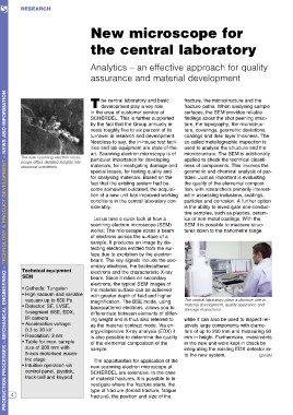
The new scanning electron micro- art. Scanning electron microscopy is of microstructure. The SEM is additionally
scope offers detailed insights into particular importance for developing applied to check the technical cleanli-
structural conditions. materials, for investigating damage and ness of components. This involves the
special issues, for testing quality and geometric and chemical analysis of par-
for analysing materials. Based on the ticles. Just as important is evaluating
fact that the existing system had be- the quality of the elemental composi-
come somewhat outdated, the acquisi- tion, with researchers primarily interest-
tion of a new unit has improved working ed in assessing inclusions, coatings,
conditions in the central laboratory con- particles and corrosion. A further option
siderably. is the ability to investigate non-conduc-
tive samples, such as plastics, ceram-
Let us take a quick look at how a ics or non-metal coatings. With the
scanning electron microscope (SEM) SEM it is possible to measure struc-
works: The microscope scans a beam tures down to the nanometre range,
of electrons across the surface of a
sample. It produces an image by de-
tecting electrons emitted from the sur-
face due to excitation by the electron
beam. The key signals include the sec-
Technical equipment ondary electrons, the backscattered
SEM electrons and the characteristic X-ray
beam. Since it relies on secondary
• Cathode: Tungsten electrons, the typical SEM images of The central laboratory plays a decisive role in
• High vacuum and variable the material surface can be achieved material development, quality assurance and
with greater depth of field and higher damage inspections.
vacuum up to 650 Pa magnification. The BSE mode, using
• Detector: SE, LVSE, backscattered electrons, allows you to while it can also be used to inspect rel-
differentiate between elements of differ-
5-segment BSE, EDX, ing weight and is thus also referred to atively large components with diame-
IR camera as the material contrast mode. Via en-
• Acceleration voltage: ergy-dispersive X-ray analysis (EDX) it ters of up to 200 mm and measuring 80
0.3 to 30 kV is also possible to determine the quality
• Resolution: 3 nm of the elemental composition of the mm in height. Furthermore, investments
• Table for max. sample sample.
size of 200 mm with in the new unit were kept in check by
5-axis motorised eucen- The opportunities for application of the
tric stage new scanning electron microscope at integrating the existing EDX detector in-
• Intuitive operation via SCHERDEL are extensive. In the case
control panel, joystick, of material fractures, it is possible to in- to the new system. (gtn/dk)
track-ball and keypad
vestigate where the fracture starts, the
type of fracture (forced fracture, fatigue
4 fracture), the position and size of the